Winter 2009
Our objective
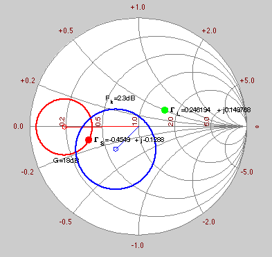
was to design, build and test a stable RF amplifier to operate in the
1.93 to 1.99 GHz frequency band. The amplifier had to have an overall
gain greater or equal to 18dB, minimum noise figure less than or equal
to 2.3dB, and input and output return loss greater than or equal to
10dB. Source and load impedances were specified at 50Ω. We were able to
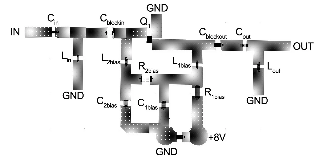
use software such as ADS to simulate the desired specifications then
build the actual amplifier on a PCB.
This project is very tricky. More often
than not, the simulation software contradicts the real thing and real
world factors such as coupled inductances on a PDB get in the way of
producing gain. In my class, my group was the only one to successfully
build an amplifier- other groups ended up with attenuators and
oscillators instead.
In general, the amplifier performed
nearly to our expectations. The fact that we were able to get an
acceptable gain of 10dB, while still below spec, was very promising. The
implementation could be tweaked further to improve the results somewhat
beyond what we were able to achieve. Designing the amplifier was a
rewarding and educational process that exposed us to the process of
designing amplifiers in real life.